| Home | Notes | Github |
|---|
Written: 22-Aug-2021
The electronics was the largest portion of this projects in several ways, from cost to lead time (because shipping from china is slow or expensive), but the design was reasonably quick1.
I thought I’d go about the design firstly focusing on the interfaces, followed by the connective tissue required to get it all to work.
The Electrical Hardware is derived from the functionality:
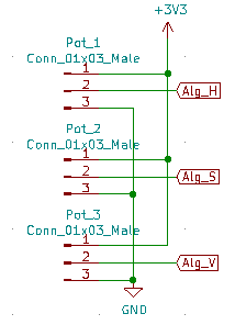
The simplest choice for the input knobs is 3 potentiometers. These create analogue signals, and thus need to be connected to ADC_IN pins. These pin locations were found using table 11 of the datasheet. I used:
| Pin #3 | Pin Assignment | Corresponding ADC |
|---|---|---|
| 11 | PA1 | ADC_IN1 |
| 13 | PA3 | ADC_IN2 |
| 14 | PA4 | ADC_IN3 |

The benefit of using potentiometer (vs using encoders) is primarily the inherent memory in the position over power cycles. The other benefit is the practical experience with ADC’s which is handy going forward.
There is only one output on the board, and that’s the 400Hz PWM signal for the RGB LEDs. WS2812Bs (datasheet) were used as they’re cheap and ubiquitous.
For redundancy I added a header for a jumper to connect to. This would connect different clock signals from the microcontroller (μC) to the LED data lines (because at this point I wasn’t entirely sure which pin I’d use / require4).
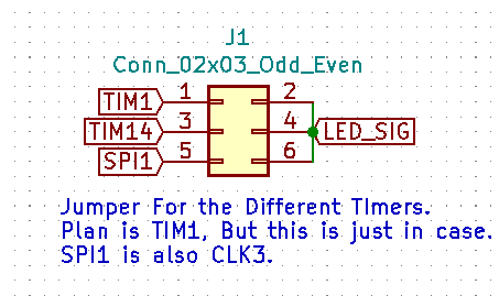
Unfortunately I forgot to actually connect these to the μC in the schematic, so this required a jumper to be added to the boards.
Fun Fact: The label only says SPI because that’s what all the datasheets called that pin. I was only interested in the fact it was attached to TIM3, but it’s fortuitous given it’s what I used in the end.
As mentioned the on-off switch was planned, and was put into the design as a simple jumper for an external switch (P_Switch1), but due to power problems it was removed.
The other issue was I didn’t know how much power the system would draw. Admittedly this could’ve been estimated, but I didn’t need to for this design5.
I wanted to run this project with an on board microcontroller (not an Arduino etc.) because I’ve never put one on a board myself, and it feels like an gap in my education.
The decision was made to go with 32 bit ARM based microcontroller (μC), even though they’re probably more powerful than I need. They’re everywhere and the skills learned mean it translates well if something more powerful is required.
Why the STM32F030C6T6? I though it prudent to learn an ecosystem, so picked STM basically at random once it satisfied the following:
STMF030 chips is cheap8, and I’d already ordered one. So using a μC that’s in the same range is pretty handy9.Step Two was to build up the basic power + programming circuity for the μC. This was done using the reference design (figure 9.) in the application notes. Portions of this circuit can be cut out, including the external clocks (as internal ones can be used).
The power of the system was intended to be fed by a micro usb port, as it’s ubiquitous and pretty safe (provided you don’t use a bargain bin wall plug thing). I didn’t manage to get it to work (as will be discussed in the issues section).
For the μC a 3.3V rail was also required. For this I used an LM1117 LDO linear regulator. This was a cheap and ubiquitous low drop out regulator used in lots of cheap 5V to 3V3 breakout boards, so was pretty confident with this part.
Beyond the already mentioned requirements I also wanted to add flexibility into the design. Why? because things were liable to not work as I’d initially expected. Safe to say a lot of this came in handy.
This gave me the following: - Link to Schematic
The design wasn’t particularly well thought through. The only things I was thinking about were keeping the connectors (mainly) to the edge, and assuming10 the current required on the 5V rail would be 1A. This meant I could use an online calculator for trace widths.
For signal traces I just kept them as thick as possible.
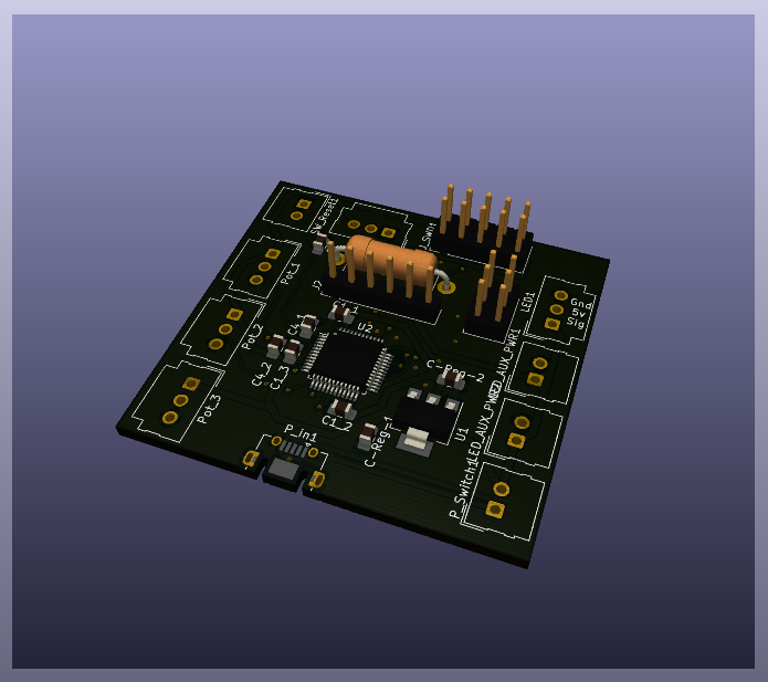
For such a critical part of the build I was rather blase about it. Trying to get this done quickly was partially to blame, but also after working out all the detail required for the μC I wasn’t too fussed about the rest. I think in retrospect the main thing was being able to get the μC to connect, and if that worked I’d have considered the whole thing a success. And by that measure this project was a success. To my surprise I even got a functioning light out of it11!
Construction of the board (excluding issues) was pretty reasonable. Soldering required patience, and liberal amounts of both flux and solder wick to make it pretty.
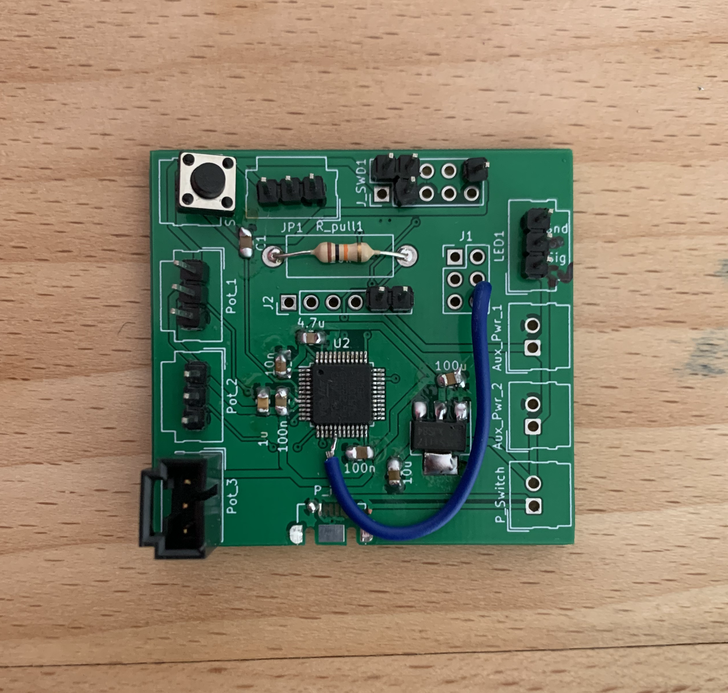
The main challenge was adding a jumper to connect the signal out from the chip to the LEDs. This was my first board:
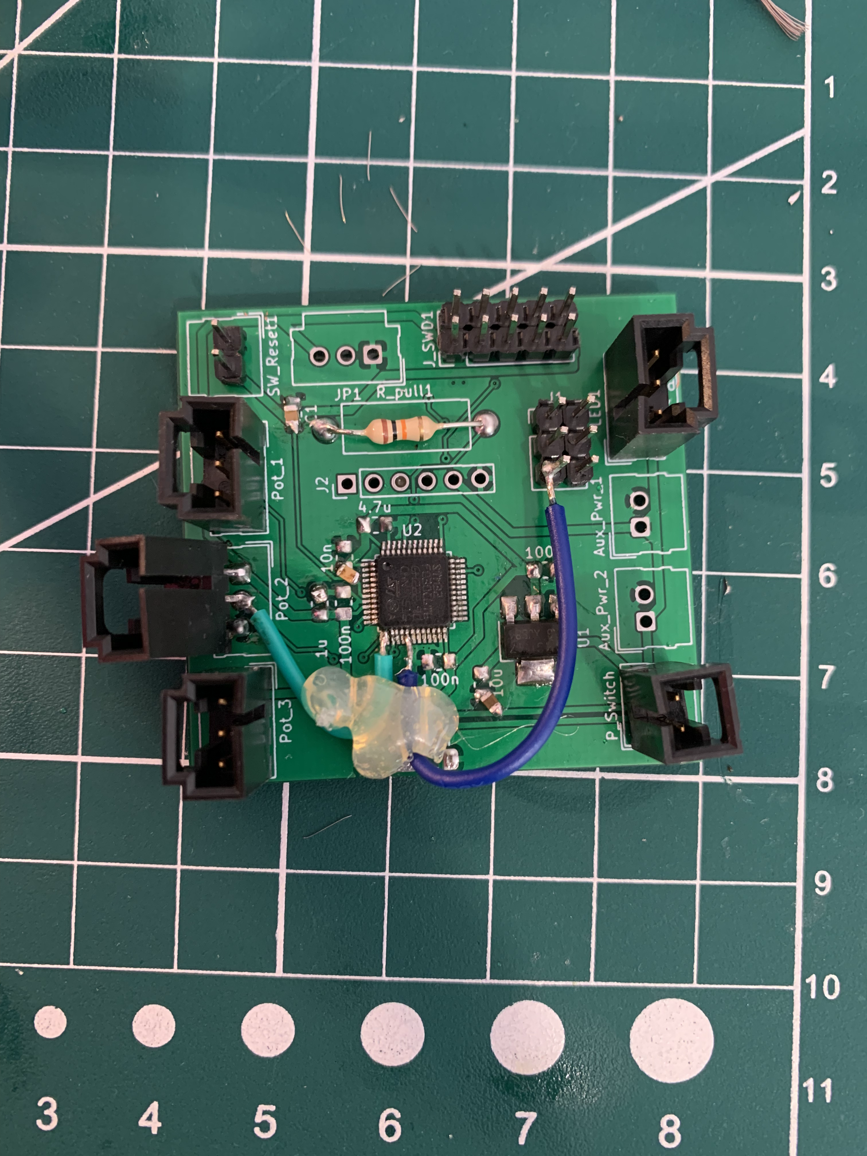
This was then re-enforced with hot glue12 as can be seen. This is the final board I ended up using
 T
T
More things to note from my first board: - R_pull1 was given a generous footprint to say the least. - The re-set switch was not the one I’d planned on using to say the least, not that it’s strictly required. - I got the silk screen wrong for the LED1 header, and corrected it in sharpie.
At this point the majority of the electronics build prior to full integration was complete. Before the next section it’d be good to talk about some problems faced with the PCB…
For a current list of issues, or - more excitingly - to add some of your own, don’t hesitate to look at the github issues page.
The first board was soldered up and in my excitement I soldered all the components. This was a mistake. When i tried to connect to the board after a second the regulator stated smoking13 and the the solder for the heat-sink pad started melting.
This fried both the regulator, and I think the μC.
Luckily everything comes in packs of 5, So I soldered another board with just the power components, and wasn’t getting the correct voltages in or out of the regulator. I thought this might be to do with one of several reasons:
The capacitor inrush didn’t seem to be a problem, because after unsoldering all the capacitors I was getting the same reading
The USB negotiation isn’t required at low power, which is all that’s needed for just the power module. This could14 still pose an issue though when trying to power the LEDs.
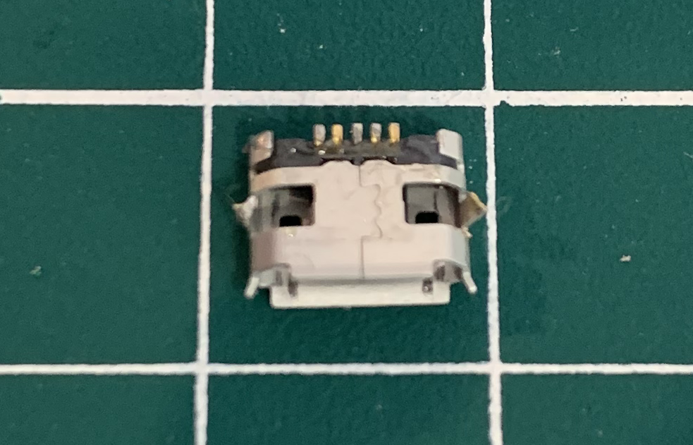
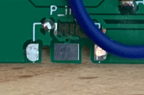
This just leaves the bad soldering. This is likely the case, because I’d bought the wrong micro-usb housings. I think this is the biggest issue with buying random components of ebay: you don’t have good data sheets, and don’t know footprints etc. As such the ones I bought could be bodged into place. he soldering was hard and risky15, and potentially too hard so for me. When I moved away from the USB power I cut the housing off and the pads came off, with the pins suggesting the solder joint was fine, but it might have been bad for any number of reasons. Pardon the low resolution.
These problems all went away when I used a breadboard 5V supply. Which was enough to program the board. In the end I used a USB to barrel jack cable which I cut and soldered onto the board on one of the spare LED power connectors. In future I think I’ll just slap a barrel jack on it and leave it there.
Possibly too quick, esp. judging by the number of issues it resulted in. however these issues might also just be difficult to solve then and there because turnaround time for all the parts was slow and expensive.↩︎
In the end I didn’t use an on-off switch due to power problems.↩︎
For a LQFP 48 Chip, as the μC here is.↩︎
Due to large lead times it was important to get the PCB out before beginning prototyping on the DISCO board, and hence my lack of knowledge going into the PCB design.↩︎
There could potentially be future iterations, but either way they’ll probably only be digital prototypes.↩︎
The ST branding for an MCU with a Cortex M0 core.↩︎
Well it’s beyond perfectly good, it’s got loads of unused potential, but anything more would be overkill.↩︎
Possibly because - as I later found out - it has been discontinued.↩︎
Very handy in fact. The code was basically copy + pasted over.↩︎
Never a good idea to assume things. As said power consumption could’ve been calculated. I think it worked out in the end though.↩︎
Somehow. I blame the sheer amount of redundancy built in plus a little sprinkling of prototyping ability.↩︎
Its not a proper project without hot glue 🧑🔧.↩︎
Bye bye magic pixies 🧚↩︎
Some chargers just give power until they cant give no more. But I’m not sure.↩︎
If the solder got into the plug itself there was no getting it out.↩︎